
Another crazy electronics project has landed. Now, I’ve got a ESP32 doorbell circuit with a few extra bells and whistles.
It started out as the simple idea of having individual doorbell buttons for me and my kids so they don’t need rushing to the door just to realize that the visit was for me.
Using ESP32
I ended up designing a circuit around the ESP32 WiFi module WROVER-B, adding a couple of peripherals for enriched functionality.
The entire project is open sourced at github.com, both hardware and firmware can be found there.
At the time of writing, the feature list is still growing. Right now it amounts to:
- Two-button interface with led indicators
- Personalized doorbell sound from custom wav files
- Cron calendar for scheduling sounds down to one second resolution
- SD card support for storing audio files and configuration
- WiFi interface with integrated antenna
- MQTT support for smart home integration and push notifications
- Battery backed-up real-time clock
- Time automatically set over the network using NTP
- Can be configured to use custom time zones
- Silent mode with alternate bell sounds during night hours
- Relay for triggering external doorbell along with custom sound
- Accepts AC or DC power input from existing doorbell power supplies
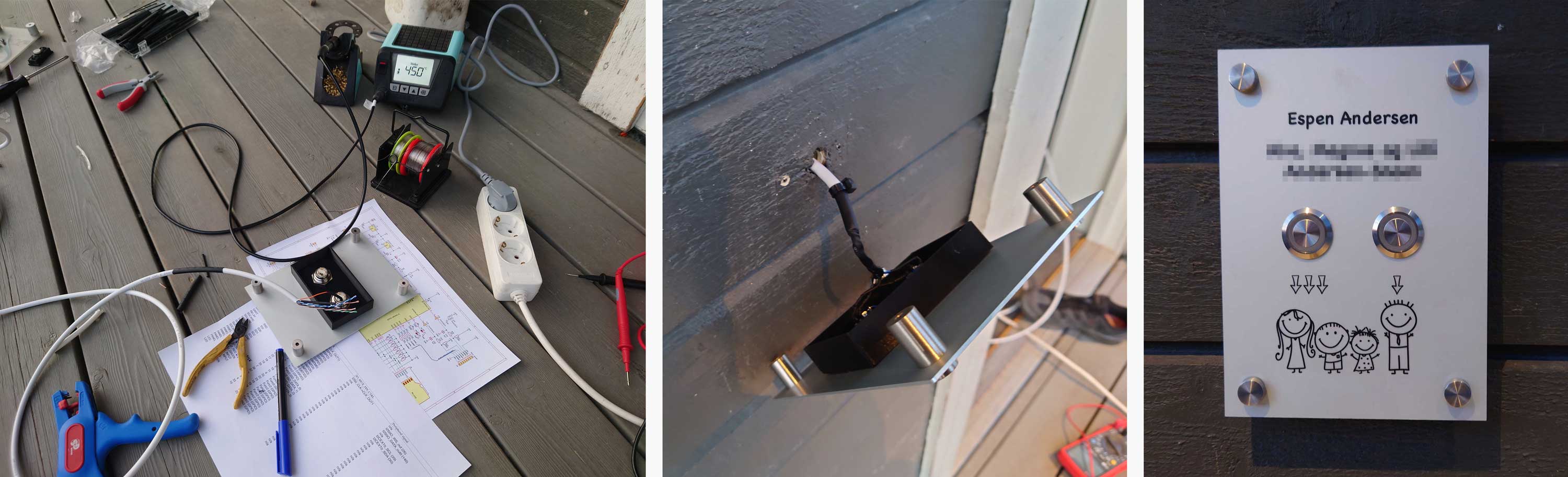
The button panel itself was made from a pre-ordered aluminum sign intended for wall mount, with standoffs to hold the sign 19mm out from the wall. I designed and ordered mine from skiltmax.no.
The right buttons
Upon arrival, i drilled the mounting holes and fit the buttons. I went for high-quality push buttons with built-in LED lights.
A note about my choice of WiFi module: The WROVER-B has been superseded by WROVER-E and is no longer recommended for new designs. Since I happened to have a number of WROVER-B modules lying around, I decided to use them for this project anyway. The E model is close to a drop-in replacement for its predecessor – at least as far as I’ve been able to clarify – so I assume there will be few problems switching to the newer version at a later time.
Initial attempts
I use KiCAD for my electronics projects. This is a wonderful open-source application that have become a very capable alternative to commercial Electronics Design Automation software.
The schematic went through a couple of iterations after some trial and error. The documentation for the ESP32 modules are excellent, but still complex. My first attempt at hooking up the WROVER was not successful at all, because I missed out on crucial details.
I failed in assigning the correct GPIO pins from the WROVER module after misreading some of the pin functions.
Specifically, I did not realise before after sending the PCB to production that – despite being labeled both in the documentation and on the module’s silk screen – certain GPIOs were not exposed at all but reserved for internal use within the module.
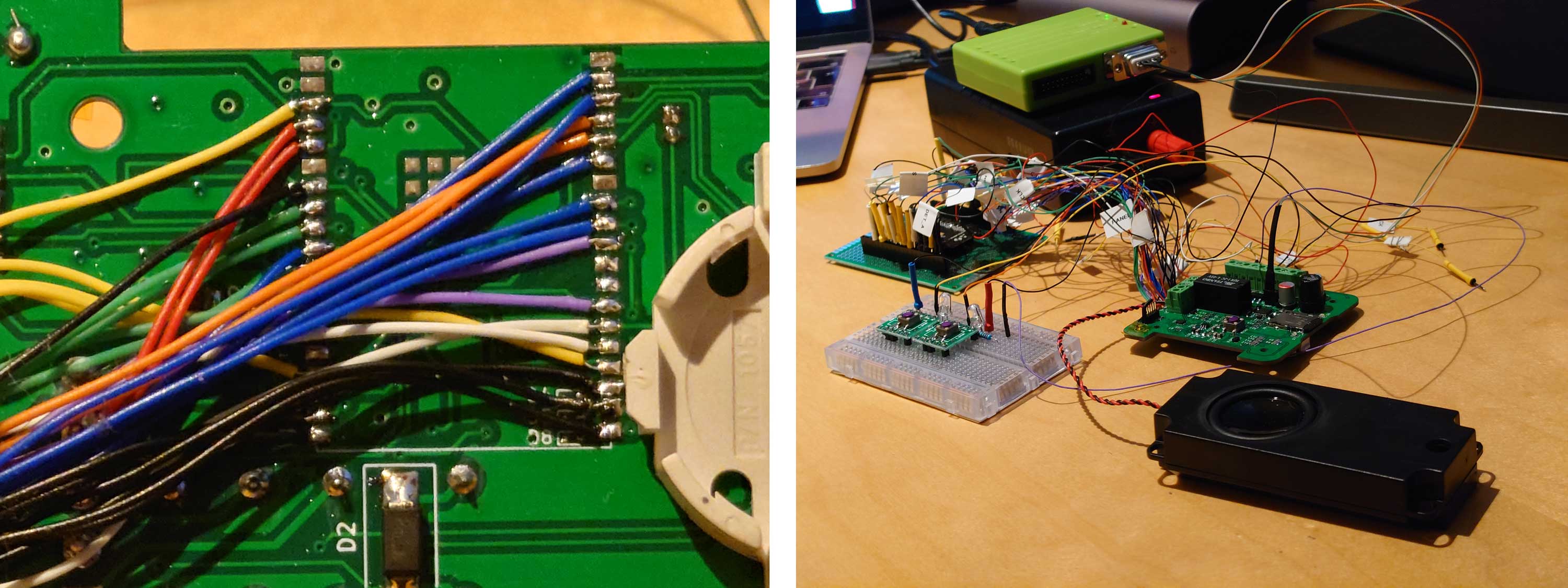
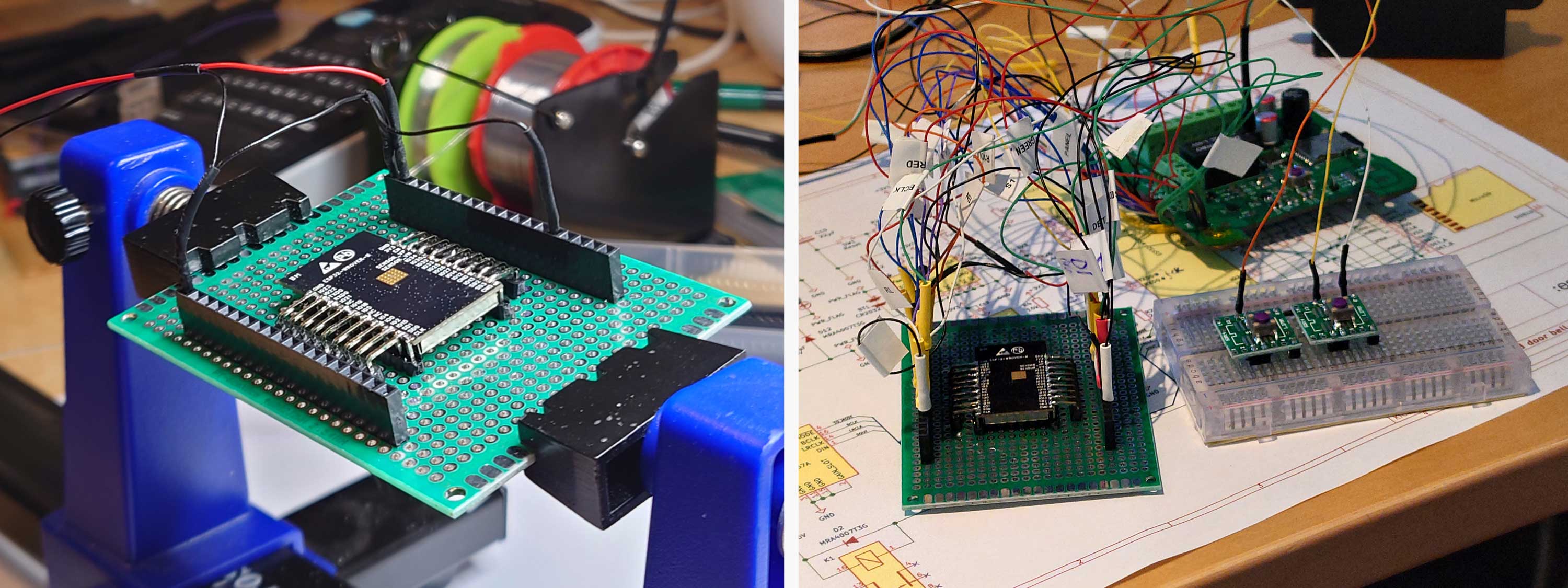
Never the less, the malfunctioning PCB did a pretty good job as a development board. I took the time to solder patch wires to the WROVER module’s footprint and put together a simple, patchable test version of one of my WROVER modules.
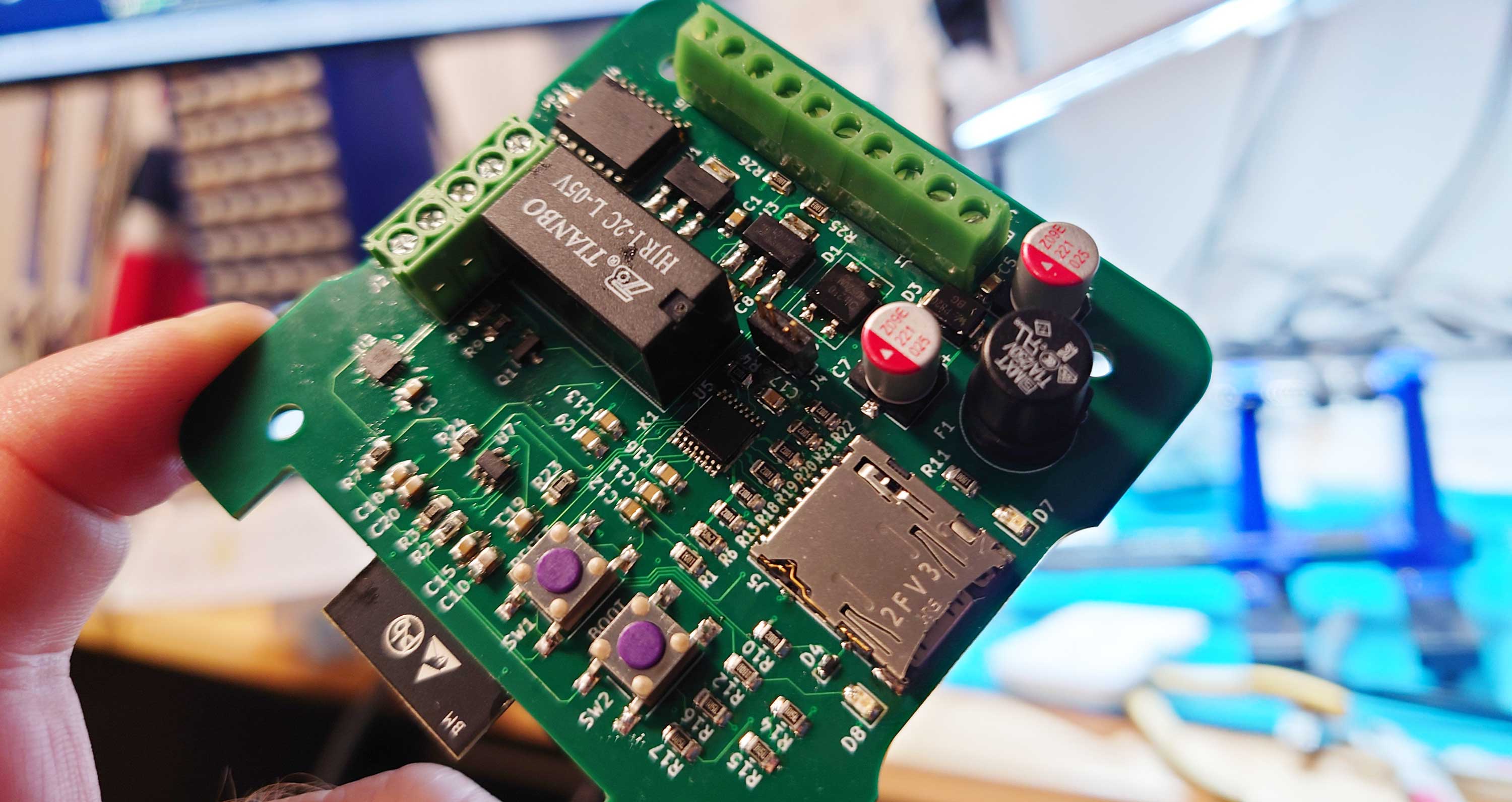
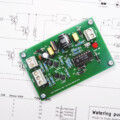
The doorbell circuit
The second attempt went much better. Below is the schematic from which I produced the new PCB.

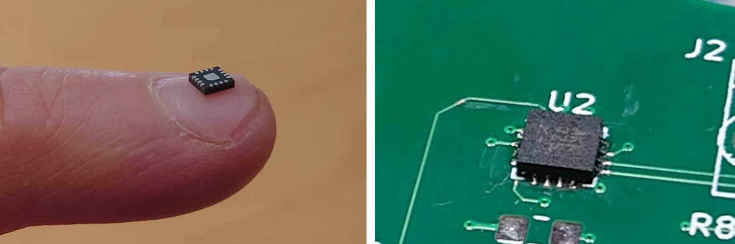
The configuration and audio clips is stored on the micro SD card (J5) connected to the ESP32 module (U6) through the SPI bus. Playback of wav-files goes over the i2s protocol to a MAX98357 audio amplifier (U2), delivering up to 3,2 Watt to a 4Ω speaker.
The circuit also has a DS3231 real-time clock (U4) with battery backup to keep track of the time schedule. It communicates over the i2c bus, and the system kicks the ESP32 real-time back in sync every 5. minute.
The doorbell circuit has connections for two push buttons and up to four LEDs for the door panel (J6). Both external buttons is connected to hardware debounce circuits that protects the microcontroller IO. These are based on two Schmitt triggers (U7A and U7B).
The ESP32 also interfaces a relay (RL1) meant to trigger a traditional doorbell, if present.
Powering the doorbell circuit
The doorbell circuit has two power rails regulated by (U1) and (U3). A 5V rail supplies the relay and the audio amplifier. A 3v3 rail supplies the WROVER and the rest of the peripherals.
The bridge rectifier (D1) allows for connecting the circuit to AC power supplies commonly found in existing doorbell units – as well as regular DC supplies. Power input may be either AC (5-8 V) or DC (7-10 V).
The circuit is protected by a 250mA slow-blow fuse. The power supply must have a high enough current rating to handle the total load.
Keeping a close eye on the input voltage is important in order to keep the primary 5V linear regulator (U1) from overheating, especially when feeding in AC. When rectified, the resulting DC voltage is about 1,4 times higher than the AC (RMS) voltage.
If the doorbell transformer delivers 8 VAC, you will end up with 11,2 VDC after rectification. Thus the 5V regulator has to dissipate enough power to maintain a 6,2v voltage drop which amounts to some temperature rise in case of maximum current draw (running wifi and loud sound playback simultaneously).
The docs for the 5V 1117-regulator I use specifies a maximum input of 20 volts. That input voltage would require heavy temperature relief, far beyond what the PCB copper fill alone provides. Therefore, an AC input of more than 8 volts is not advisable without proper cooling of the regulators.
There are two on-board push buttons. Reset (SW1) and boot (SW2). The reset button restarts the microcontroller and the RTC. The boot button puts the WROVER in download mode if pressed during reset.
Programming
Programming the doorbell circuit takes place over UART0 on the ESP32. The WROVER’s 3v3 logic level is converted to ±5V level by a MAX3232 chip. The UART pins can hence be connected directly to any RS232 compatible interface.
I use a Flyswatter 2 programmer, providing a USB-to-serial interface that works well with this configuration.
The firmware for the doorbell circuit is written in C++, using Espressif’s own IDF framework along with the FreeRTOS operating system.
For time scheduling, I use ccronexp from staticlibs, a fantastic library that brings the power of cron expressions to your microcontroller. Pair this library with the power of a battery backed-up real-time clock like the DS3231 chip, and you got a winning combo.
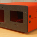
Designing the PCB
The ever so difficult task of finding a nice enclosure must be landed before starting on the PCB design. I decided to go for a nice, wall-mounted white 76×76 mm vented cube from New Age Enclosures.
The data sheet for the enclosure is very accurate. It even suggests a cut-out for the PCB.
I drew the board profile in QCAD, and imported the resulting DXF file directly into the edge.cuts layer in KiCAD.
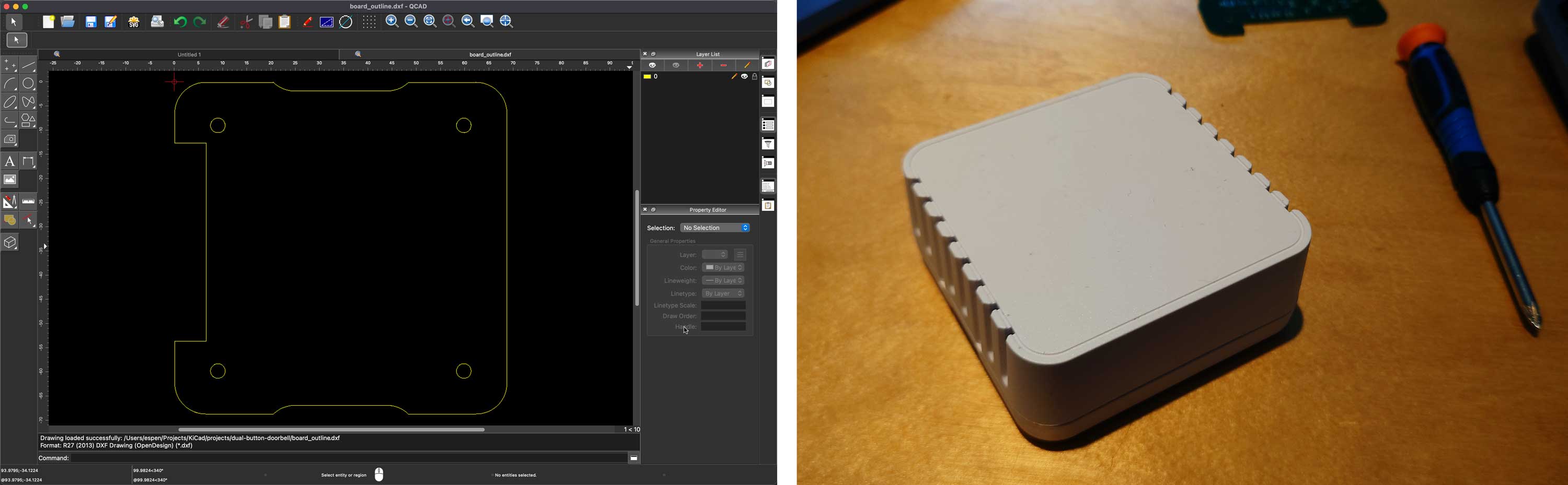
The design is moderately dense and a four layer board seemed like a natural choice. Top and bottom layers for signals and the inner layers for power planes.
Part placement
Once the outline is in place, the parts can be laid out on the board surface. Part placement is probably the most important stage of the PCB design process.
This is where your schematic diagram meets the hard realities of the real world in terms of limited space, demand for short wire lengths, logical placement of user interface components and various other physical constraints.
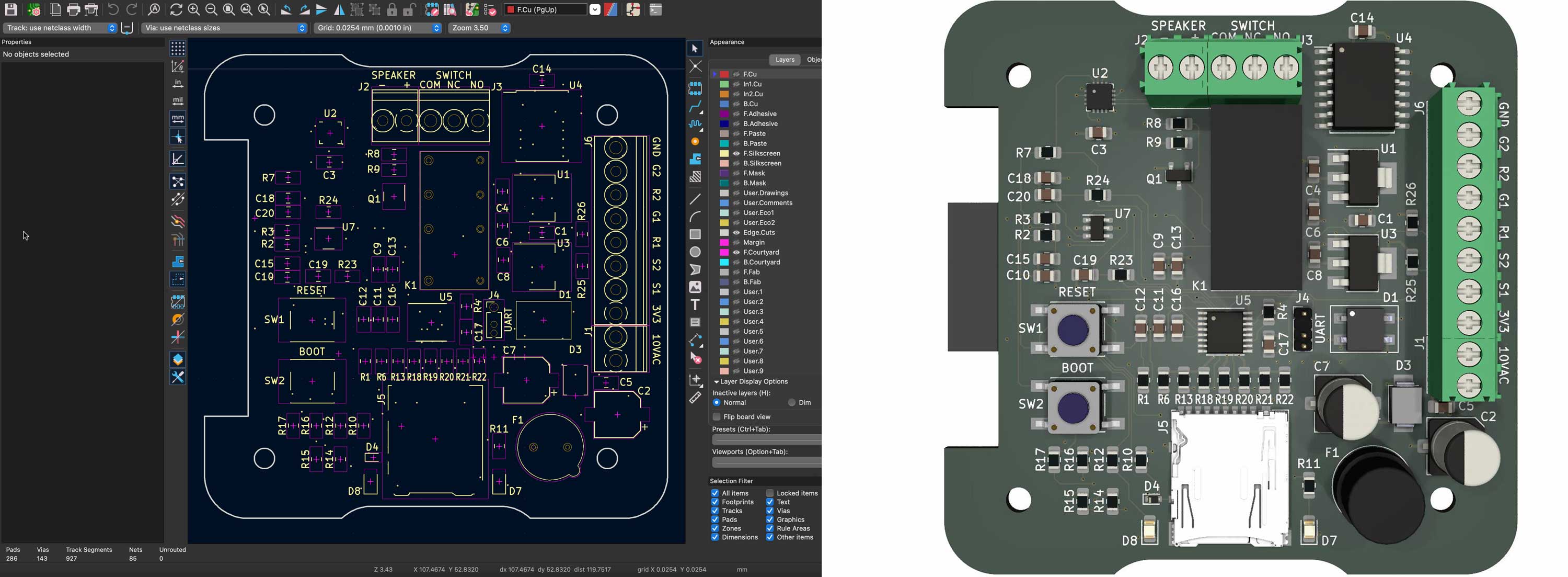
KiCad has a built-in 3D viewer that renders a life-like image of the PCB. After placing the parts, I always use the 3D viewer to check and adjust the positioning of components and silk screen labels.
While most of the 3D-models used are already in KiCads default component libraries, some of them had to be downloaded from sites like grabcad.com or snapeda.com. Other models, such as the SD card holder, could be found on vendor web sites.
A few parts needed to be designed from scratch using FreeCAD. These are available from my profile on GrabCad.
The 3D viewer makes it easy to keep an eye on the aesthetic qualities of the design. I always try to keep components aligned and evenly distributed across the board area.
I arrange the silk screen labels so that they are fully visible and in non-ambiguous positions.
Routing
Now, routing of the board can begin. I like to do away with the longest tracks first. I flip them to the back side of the board and route them across to their destinations while trying to keep them together as best I can.
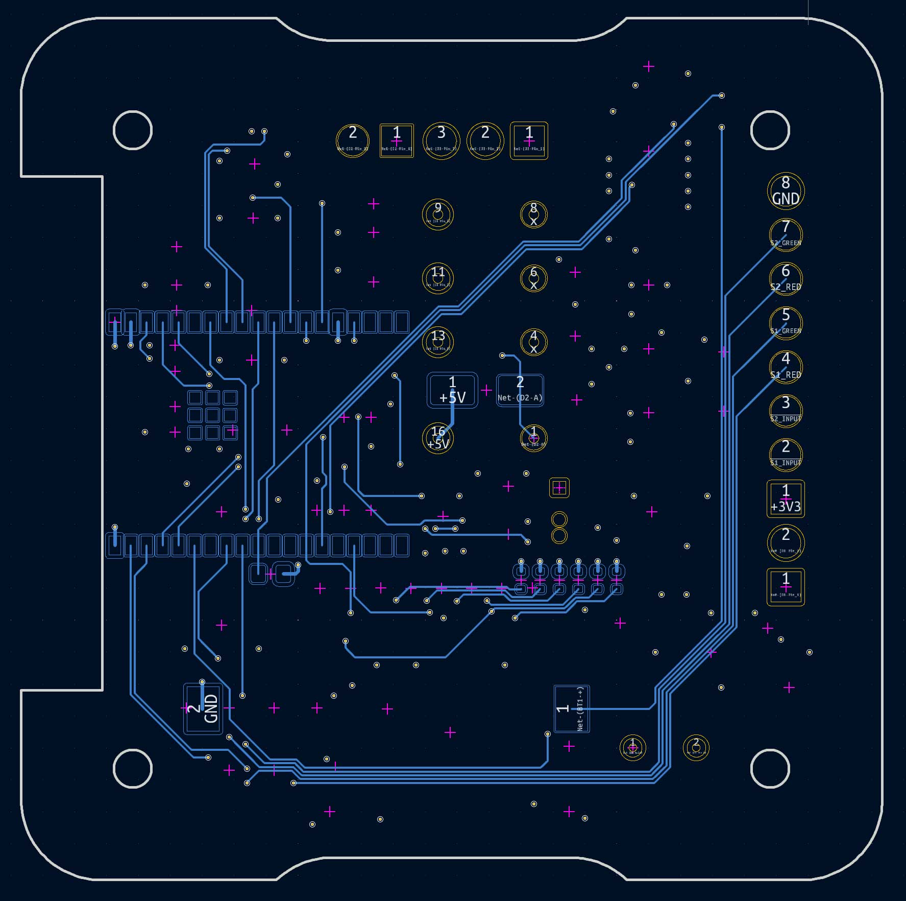
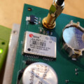
I like to keep as much of the signal wires at the top layer as possible, using the bottom layer mostly for the longest traces. The WROVER module is placed on the bottom layer as well, along with the holder for the CR2032 backup battery for the real-time clock.
The bottom layer holds a few additional components that didn’t make it to the top layer. The design would simply get too crammed for hand soldering if I’d gone all in on putting everything at the top side.
Ready for doorbell production
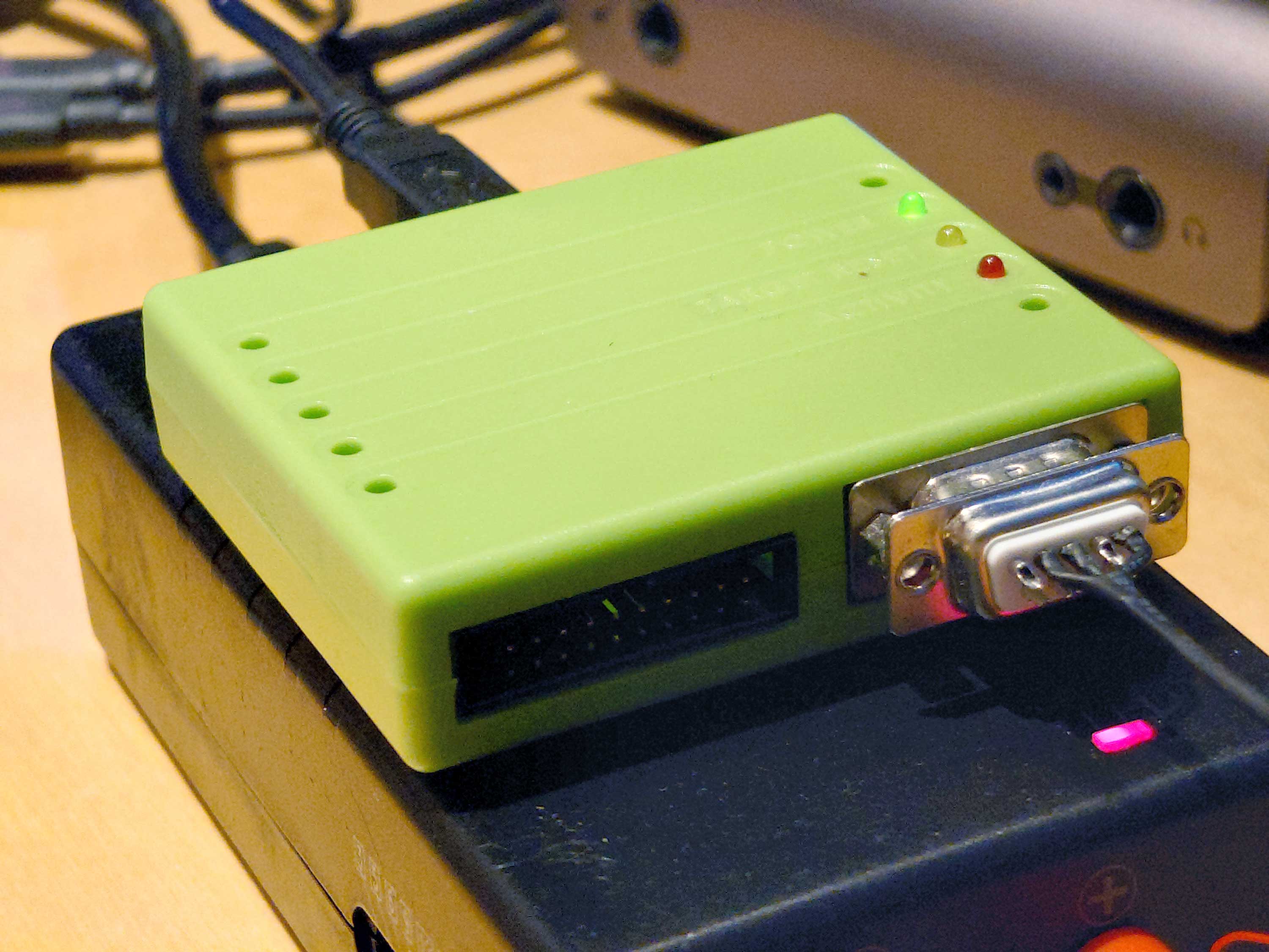
This is where my home made development rig really came into play. When working on the board, I sometimes wanted to move connections from one GPIO pad to another to improve routing.
First, I did the changes on the development board, updated the firmware and tested if it still worked. Then I went back to the schematic editor and made the edit. Finally, i pulled the changes into PCB editor and re-routed the relevant traces for the doorbell circuit.
After creating the PCB in KiCad, the board is ready for production! I use JLCPCB to make my boards. They are very reasonably priced, and the boards typically arrive at my door about a week after submitting the Gerber files.
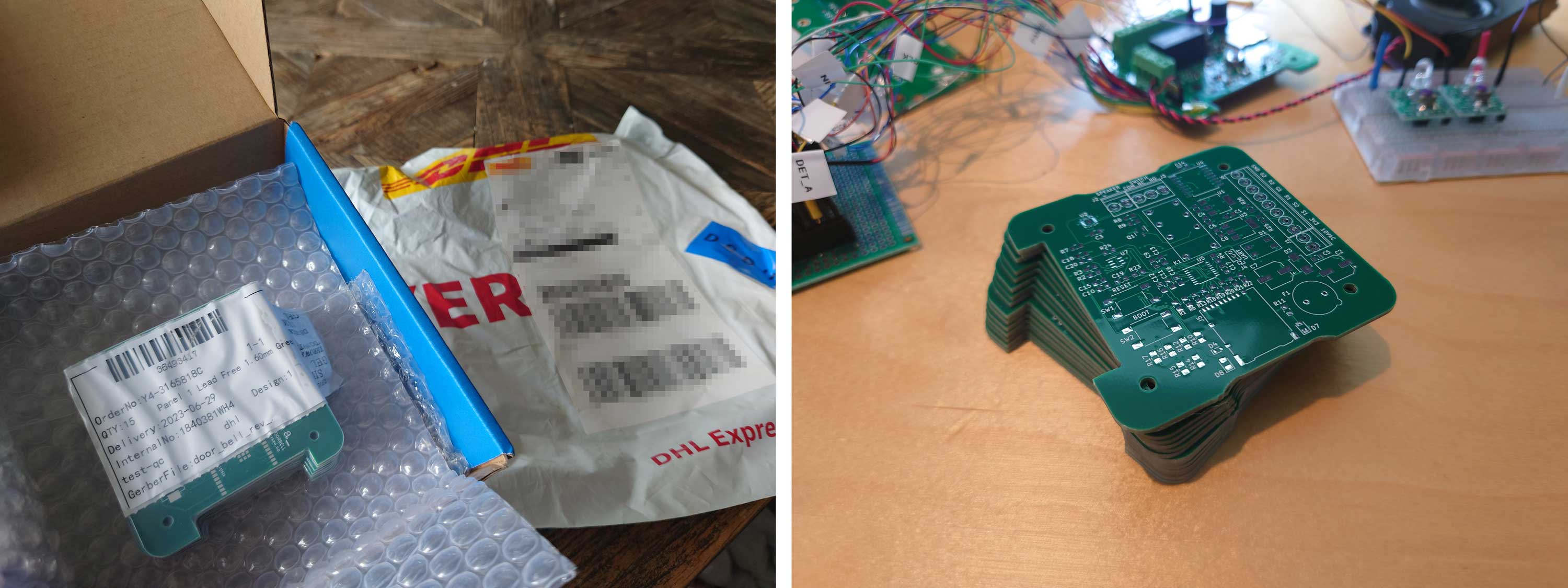
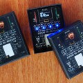
I got 15 copies of this second version of the PCB, feeling confident that this time, I got things right.
Soldering and cleaning
Hand soldering SMD components takes a bit of practice. Some packages are quite easy to do, others more complicated.
The MAX98357 sound amplifier is delivered as a QFN-16 package. That’s 16 connections distributed around a 3x3mm chip.
Still, with the right tools, steady hands and a considerable amount of flux, it’s absolutely doable. There are a number of videos on YouTube, describing how to solder small SMD packages.
I usually start out by soldering the smallest packages first. If the board gets too crammed up, the smallest footprints can be hard to reach from a proper angle.
After the solder works, the PCB is cluttered with flux. Therefore it needs to be thoroughly cleaned, and for that I use Isopropyl Alcohol (IPA) and a baby toothbrush.
Note that you should use the high quality type of IPA specifically intended for use on electronics, not the cheap one you get from a hardware store.
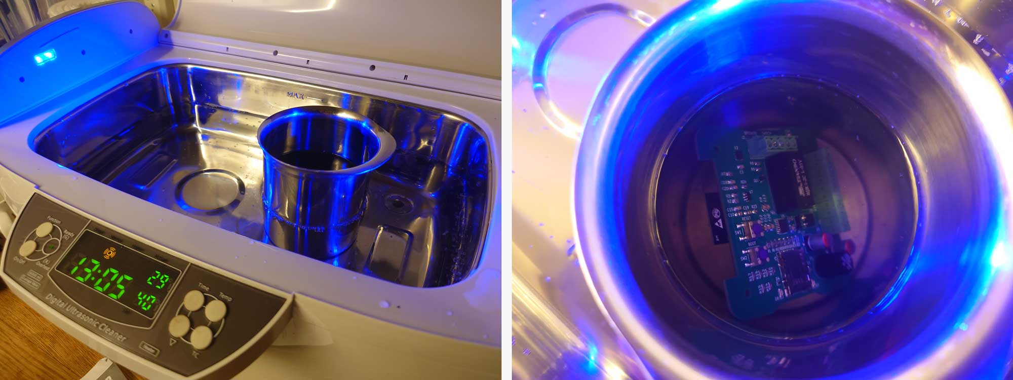
After brushing off soldering debris and flux with IPA, I then give it a few minutes in an ultrasound washer, which is very effective. Use an appropriate cleaning agent for electronic works.
I take care not to run the washer for too long. The tiny parts within the ESP32 module is prone to damage from the mechanical stress imposed by prolonged exposure to ultrasound.
Mounting the doorbell
After drying up, the PCB is ready for mounting. I use nylon screws for fastening the board inside the enclosure. I also needed two 5mm standoffs to lift the board a bit up, to make room for the ESP32 module and the RTC battery.
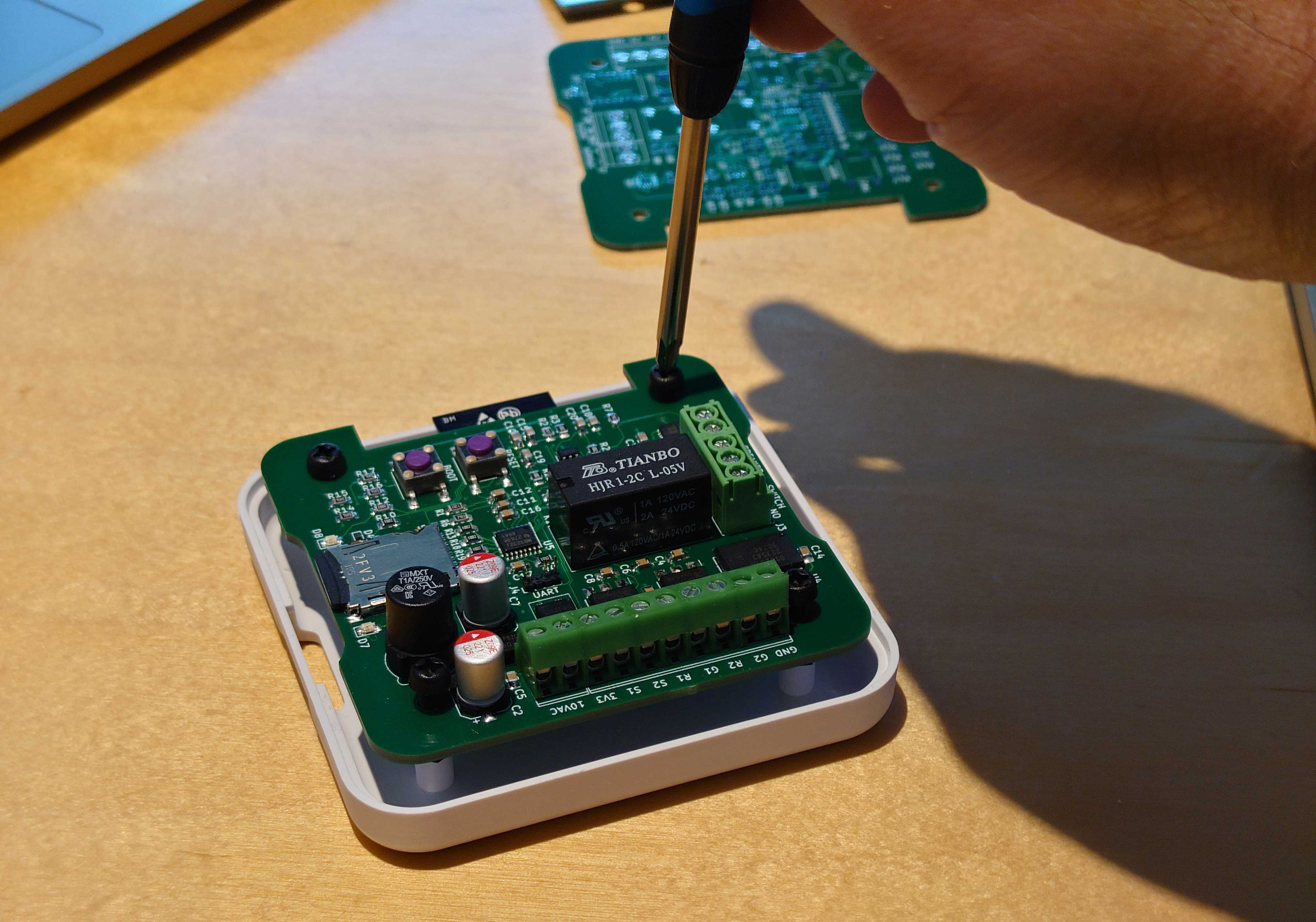
Programming and testing the new PCB went well, so the next step is to get it up and running.
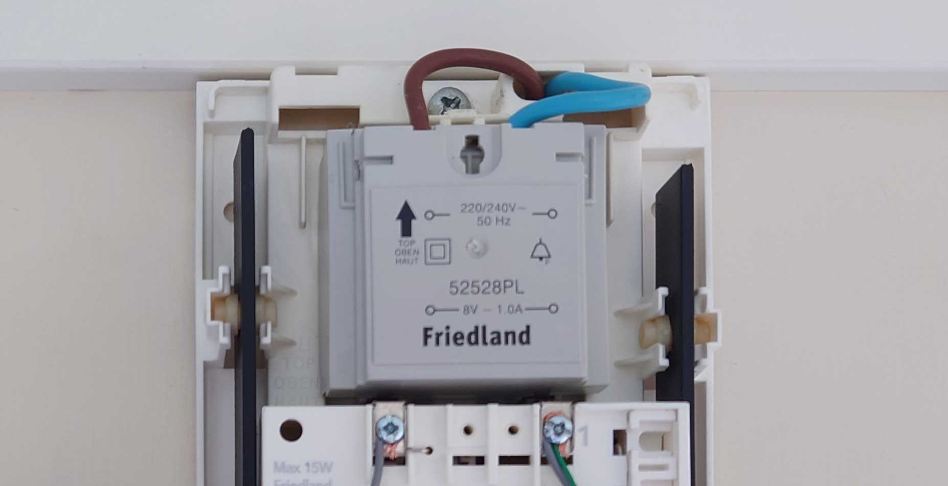
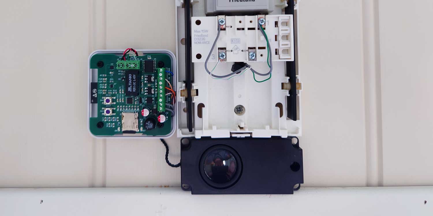
I use the existing low-voltage output from the doorbell transformer. The power connection and the wires form the door panel connects to the right terminal block according to the schematic.
Before connecting the power leads, i removed the fuse (F1), to prevent any mishaps while fiddling with the wires.
The speaker and the wires normally going to the ESP32 doorbell switch is connected to the upper terminal block.
This is an incredibly impressive project! I really enjoyed how you documented every stage from the initial idea to the final wall mounted installation. The detailed explanation of your schematic design power regulation and GPIO challenges will be extremely helpful for anyone attempting a similar ESP32 build. Your troubleshooting process and use of a patchable development board show real engineering dedication. I also appreciate the thoughtful features like MQTT integration silent mode scheduling and custom audio support. The PCB design and enclosure planning are especially well explained. Overall this is a well executed and inspiring DIY electronics project. Great work and thanks for sharing all these valuable insights!